Microfabrication practicals
MICRO-332
Liste des groupes
TOPIC 1: Introduction TP Micro 332
TOPIC 2: AZ1512 HS photoresist thin films coating and UV exposure
TOPIC 3: Liftoff, surface preparation , and AZ nLOF 2070 negative resist
TOPIC 4: Cleanroom session
TOPIC 5: Scanning electron microscope and optical microscope characterization
In this session, students will employ both a scanning electron microscope (SEM) and an optical microscope (OM) to make distinct observations of the samples they have prepared in previous sessions. These samples are composed of negative resist AZ nLOF 2070 on silicon or glass substrates. Through these tools, students will investigate how the sidewall profiles of the resist change in response to post-exposure baking (PEB) temperature and development time. The choice of the appropriate method will vary based on the specific information looking for and the material under investigation.
1. Optical microscopy
Detecting the edges of resist patterns on substrates can be achieved using a simple method: optical microscopy (Nikon, Eclipse LV100ND). While optical microscopes offer good resolution, they may not provide detailed information about the sidewall profiles of the resist patterns, which are often the goal of this observation.
One advantage of the optical method is its convenience; samples can be easily loaded into a holder without the need for specific preparation procedures to secure them in place. Additionally, when dealing with transparent materials such as glass and nLOF negative resist, optical microscopes can be used in either transmission or reflection mode. However, when working with a silicon substrate, only the reflection mode is feasible. Furthermore, optical microscopes can leverage polarized light to extract additional information about edge profiles. The use of polarized lenses allows for differentiation between different regions of the sample with varying properties.
Mount the sample on the sample holder, ensuring that the observed patterns are positioned at the top, facing the objective. Some typical examples are shown in the following figures. When viewed in transmission mode, both edges (the top and bottom ones) are easily visible
2. Scanning Electron Microscope
The scanning electron microscope allows detailed examination of designs, assists in the development of new fabrication and production methods. The high-resolution capabilities of SEM have become indispensable in the quality control process. The information SEM provides is related to the topography, the composition, and the morphology.
The samples are examined using an SEM (Hitachitabletop Microscope, TM-1000) connected to computer for image capture. Thanks to the advancements in electronics and new techniques, this machine has become more accessible for many users, requiring only a short training period to operate effectively. However, achieving sharp and informative photos necessitates proper sample preparation and SEM parameters optimization.
Sample Preparation
- First, it is important to consider the sample’s size, its shape and state, and its conductive properties.
- For the observation of the cross-section of the patterned resist, the sample must be accurately cleaved along the specific area for analysis. Since cleavage is a manual operation, success is not guaranteed, and it must be performed with careful precision, often requiring repeated attempts.
- The appropriate sample position for SEM observation is achieved using a specialized holder, which allows the sample to be positioned at a tilted angle.
- Mount the sample on the sample holder and orient it at an angle, ensuring that the observed patterns are positioned at the top, facing the electron beam.
- From these digital SEM micrographs, determine as many shape parameters as possible, including width, height, and the angle of the sloped sidewalls, as illustrated in the following figure.
Following are SEM images of nLOF resist on silicon substrate with sloped sidewalls.
TOPIC 6: Electrical and optical characterization
1. Objective
During this laboratory, you will learn how to use the four-point probe device for electrical characterization of aluminum thin film and an optical microscope to measure the dimensions of patterns and alignment errors.
a. Alignment errors
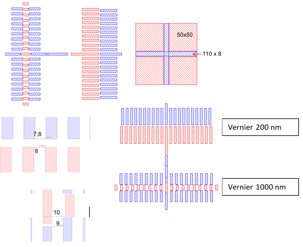
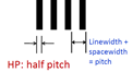
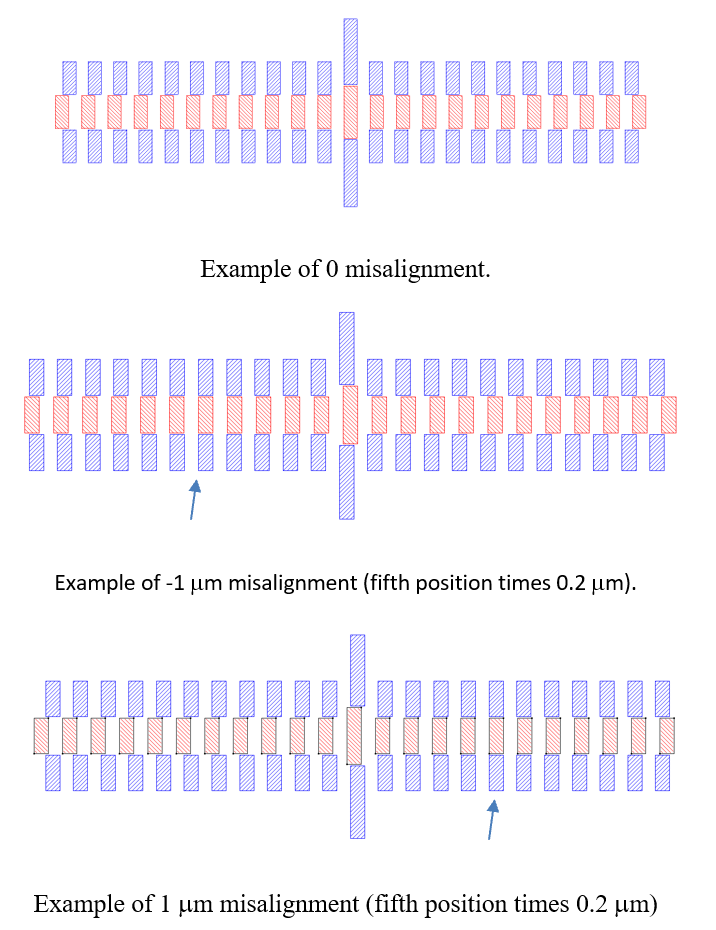
This procedure is used to determine alignment capability using Vernier scales. They are patterns designed to resolve alignment errors for a given process. Figure 1 shows a vernier design. The blue structure has lines that are 4 µm wide and spaces that are 3.8 µm wide ( resulting in a pitch of 7.8 µm). The red structure has both lines and spaces which are 4 µm wide ( the corresponding pith is 8 µm). The difference between the two structures pitch, 0.2 µm, is the resolution of the vernier. A perfect alignment is obtained when the central lines (long lines) are well aligned. In case a misalignment exists, find where the first red and blue lines are aligned and count its position from the long line. The misalignment is the position number times the offset, 0.2 µm. A second vernier with a resolution of 1 m is added in case where error alignement is very large.
The pattern of the vernier in your mask with features size are as follow:
Figure 1: layout of the Vernier, in red is level one and in blue is the level two. The two levels are shown superimposed.
b. Measurement Procedure
Under the optical microscope (Keyence digital microscope), observe your wafer in which you have already aligned the second-level photoresist on the patterned first-level wafer (in the cleanroom session).
- Each student characterizes a vernier located at (x,y) position.
- Inspect the vernier on the wafer and take a picture.
- Record misalignment errors for x and y positions at different locations on the wafer:
|
Student name |
|
|
|
|
|
Vernier coordinates (x,y) |
(0,28) |
(28,0) |
(-28,0) |
(0,-28) |
|
Dx ( unit ) |
|
|
|
|
|
Dy ( unit ) |
|
|
|
|
- Observe under optical microscope, your wafer with aluminum patterns obtained by the etching process and the one by lift-off process.
- Take pictures of the same pattern with the same magnification.
- Measure their dimensions.
- Inspect and compare the difference between the patterns obtained by the two methods.
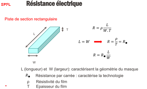
3. Electrical characterizatio
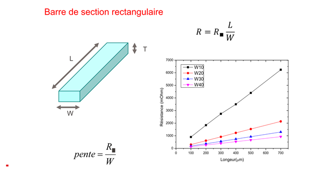
3.1. Transmission line method (TLM)
Resistors are tested and characterized with Karl Suss PM6 Probe station and the Keysight 34420A Nano_Volt/Micro_Ohm Meter. The devices to be tested are aluminum resistors obtained by chemical etching and lift-off methods. The layout of the resistors is shown in figure 2.
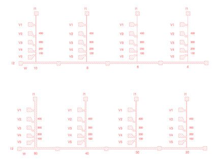
- These structures will be used to plot the curve R versus L, where R is the electrical resistance and L is the length of the resistor segment.
a. Measurement Procedure
Place the sample on the wafer stage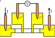
- Place the probe tips on
the contact areas as follows:
- ·Two probe tips for current injection, these probes are labeled I1 and I2. Under the optical microscope, use the micropositioning stage to place each tip on the corresponding pad on your sample with the same label of the probe tip.
- Two probe tips for voltage measurement with labels V1 and V2. Under the optical microscope, place each tip on the corresponding pad on your sample.
- Select the 4W mode on the Keysight 34420A Nano_Volt/Micro_Ohm Meter, the resistance value is directly displayed.
- Complete the following
table:
|
contact |
V1-V2 |
V1-V3 |
V2-V3 |
V2-V4 |
V3-V4 |
V4-V5 |
W (unit) |
Student name |
|
L(mm) |
400 |
750 |
300 |
550 |
200 |
100 |
|
|
|
R(unit) |
|
|
|
|
|
|
|
|
|
R(unit) |
|
|
|
|
|
|
|
|
|
R(unit) |
|
|
|
|
|
|
|
|
|
R(unit) |
|
|
|
|
|
|
|
|
- Plot R versus L and calculate the slope of the curve.
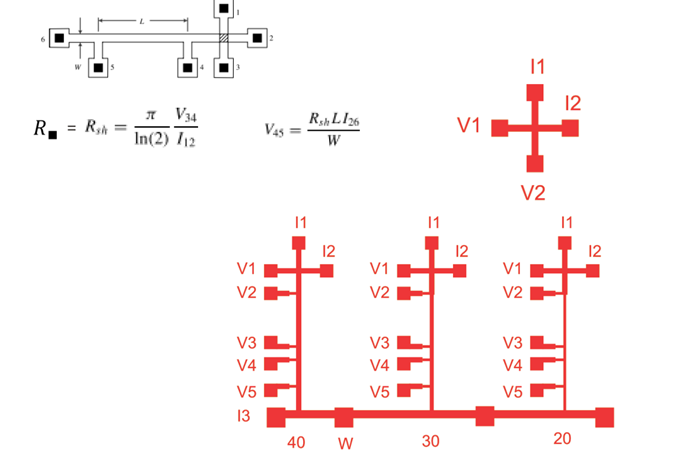
3. 2 Sheet resistance measurement
The following Structures will be used to measure the sheet resistance.
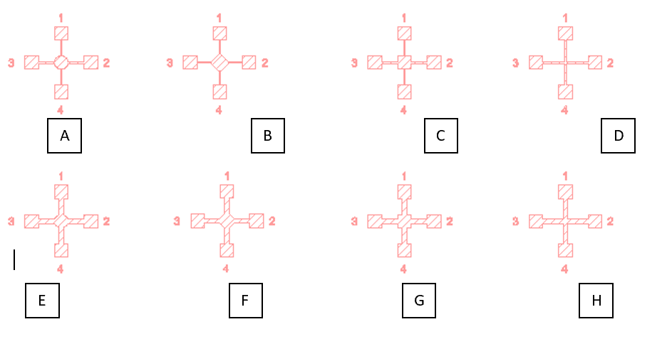
a. Measurement Procedure
- Place the probe tips on
the contact areas as follows:
- for current injection: pads 1 and 2
- for voltage measurement: pads 3 and 4.
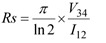
- The resistance value displayed is used to calculate the square resistance by the following formula:
- Complete the following table:
|
structure |
A |
B |
C |
D |
E |
F |
G |
H |
|
Rs (unit) |
|
|
|
|
|
|
|
|
- Compare the value of Rs for the different structures.
- From Rs and the slope of the curve R versus L, calculate the width of the measured structure.
- Compare this value to the one obtained by optical measurement.
- Compare the measured value of W to the one registered on the photomask.
- Knowing the thickness of the aluminum film (measure done in the cleanroom session), determine the resistivity of the film?